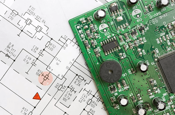
Reliable products start with repeatable assembly. Controlling soldering, component placement, and cable terminations prevents field failures, expensive rework, and compliance gaps. This guide breaks down the primary failure modes in PCB and cable harness assemblies, ties each defect to likely root causes, and lays out practical prevention steps engineering teams can apply during design, procurement, and production. You'll find how inspection tools, material controls, and DFM practices cut solder bridging, cold joints, insulation breakdown, and crimp intermittency — all while supporting flexible, high-mix, low-to-mid-volume runs. The article walks through common PCB defects, harness failure modes, step-by-step quality workflows, the benefits of US-based HMLV manufacturing, how certifications lower defect risk, and concrete DFM rules to boost first-pass yield. Wherever possible we link each failure to specific mitigations — stencil tuning, AOI/SPI strategy, calibrated crimp tooling, and environmental testing — so teams can de-risk prototypes and production launches.
Common PCB Assembly Quality Issues and How They Affect Product Reliability
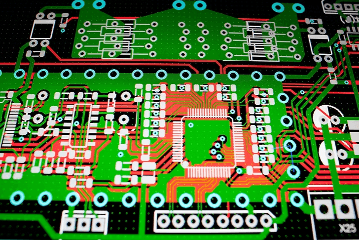
PCB assembly defects directly influence device function, safety, and total cost of ownership by producing opens, shorts, thermal failures, and intermittent faults. Typical problems — solder bridging, cold solder joints, voids, tombstoning, misalignment, and pad lifting — each create specific failure modes that inspection and testing must target. Catching issues early reduces rework and field returns, and the right process controls keep latent defects from slipping past functional tests. Understanding how these faults form informs stencil design, paste choice, and placement strategies, which we cover next.
Key PCB assembly defects and their operational effects are listed below.
- Solder bridging: Adjacent pads short together, causing functional shorts or component damage under power.
- Cold solder joint: Poor wetting creates high resistance or intermittent opens that surface under vibration.
- Voids in solder joints: Entrapped gases reduce thermal conduction and weaken joint reliability.
These failure types point directly to solder-process root causes — stencil printing, paste choice, reflow profiles, and placement variables — and to the controls (SPI, AOI, reflow profiling) that follow.
How the table works: the chart below pairs common PCB defects with typical root causes and pragmatic mitigations production and design teams can implement before release.
DefectTypical Root CausesPrimary Mitigation Solder bridgingExcessive paste, tight pad spacing, improper stencil aperture designTune stencil apertures, reduce paste volume, select paste with appropriate rheology Cold solder jointInsufficient peak temperature, poor wetting, contaminated surfacesOptimize reflow profile, improve preheat, follow J-STD-001 cleaning and handling VoidsOutgassing from paste or substrate, aggressive ramp ratesAdjust ramp/soak, consider vacuum reflow for critical BGA joints TombstoningUnequal wetting forces, asymmetric pad geometryBalance paste deposits, adjust placement spacing, update footprint DFM Pad liftingExcessive mechanical stress, delamination from thermal shockUse controlled thermal ramps, choose suitable laminate, implement keep-out zonesThat comparison shows how each defect maps to concrete process and design changes — a direct path from root-cause analysis to on-line controls and DFM improvement.
What Causes Solder Defects — Bridging, Cold Joints, and Voids?
Solder problems arise where stencil printing, paste chemistry, component wetting, and the reflow thermal profile interact. Oversized or misaligned stencil apertures deposit excess paste that promotes bridging. Incorrect ramp rates or insufficient soak can leave flux under-activated and parts under-wetted, producing cold joints or high void content in BGAs. Early detection — SPI to verify paste volume, AOI for post-reflow visual defects, and X-ray/AXI for internal voids and BGA integrity — lets teams target fixes where they matter most.
Practical fixes start with stencil aperture tuning and choosing a paste matched to component geometry, then validating the reflow profile through thermal profiling and cross-sections. Controlled paste storage and handling (temperature and humidity limits) reduce variability. For high-reliability assemblies, vacuum reflow or carefully adjusted ramp/soak profiles can lower voids. These steps set the stage for precision placement and feeder management to prevent placement-related defects.
Analysis of Solder Joint Failures During Soldering Process
This paper reviews the analysis methods used by failure analysis labs to detect, localize, and investigate solder joint failures that originate during soldering. It covers common failure modes, inspection techniques, and root-cause examples. Optical microscopy documents and locates failures; X-ray microimaging inspects hidden joints (BGA, flip-chip, CSP) and measures solder/void content; SAM (scanning acoustic microscopy) visualizes delaminations or cracks inside packages and assemblies. These tools also inspect PWB tracks and via metallization to support thorough failure analysis.
How Do Placement Errors Degrade PCB Assembly Quality?
Placement faults — offsets, rotation, tombstoning, or wrong/missing parts — usually stem from pick-and-place setup, feeder alignment, or part handling, and they immediately reduce yield and functional-test pass rates. Misaligned components can prevent proper fillet formation, cause solder bridges with adjacent pads, or induce mechanical stress that lifts pads during thermal cycling. Prevention depends on pick-and-place calibration, correct nozzle and feeder choices, and validated placement programs with feeder positional checks and vision-assisted alignment. Smart DFM — adequate pad sizes, clear fiducials, and spacing — reduces an assembly's sensitivity to small placement errors and lowers tombstoning risk.
Verification via placement-AOI and first-article inspections catches many placement issues before reflow. Cross-functional prototype reviews between CAD and process teams prevent recurring footprint or polarity mistakes. That alignment naturally leads into harness failure modes, where material and termination control are equally critical.
Which Cable Assembly Defects Matter Most for Harness Reliability?
Cable and harness failures typically show up as opens, shorts from insulation damage, high-resistance contacts from poor crimps, or mechanical breaks due to inadequate strain relief — each with distinct assembly and specification causes. Correct conductor choice, compatible insulation chemistry, and proper gauge vs. ampacity prevent overheating and chemical or mechanical degradation in the field. Precise crimping and connector handling deliver low-resistance, vibration-resistant terminations. Testing — continuity, hipot where required, pull-testing, and functional verification — confirms integrity, and design-level items like bend radius and clear labeling improve long-term serviceability.
The table below maps common harness failure modes to preventive actions and the inspections that help make quality decisions during assembly and incoming inspection.
Failure ModePreventive ActionInspection / Test Incorrect wire gauge/ampacitySpecify AWG vs expected current, temperature rating, and shieldingBOM verification, sample ampacity checks Insulation abrasion or nicksUse correct stripping tools and maintain tooling guardsVisual inspection, hipot for dielectric breakdown Poor crimp/contact deformationUse calibrated dies and tooling; train operatorsPull-tests, contact resistance, microsection cross-sections Strain-relief failureDesign mechanical clamps and enforce proper bend radiiMechanical load testing, flex-cycle testing Micro-fretting at mating surfacesSpecify proper plating and connector materialsMating cycle tests, contact resistance monitoringHow Does Wrong Wire Selection or Insulation Damage Cause Harness Failures?
Using an inappropriate conductor, gauge, or insulation chemistry exposes assemblies to overheating, chemical attack, or mechanical fatigue that leads to premature failures. For example, undersized AWG for the expected current causes heating that degrades insulation; incompatible jackets can fail under chemical or UV exposure. Correct specification matches temperature rating, dielectric properties, shielding, and flex life to the end-use environment and benefits from WHMA harness-construction guidance. Proactive sample testing — thermal aging, chemical exposure, and flex cycling — validates choices before production and informs the necessary strain-relief designs.
Those material decisions directly affect termination outcomes, where tooling and process control determine contact reliability and long-term signal integrity.
What Happens When Crimps and Terminations Are Poor?
Poor crimps raise contact resistance, cause intermittent connections from micro-fretting, and create localized heating that accelerates insulation failure — all of which degrade harness reliability. Typical root causes are wrong die selection, worn tooling, inconsistent stripping, and insufficient conductor bite that loosens under vibration. Preventive measures include calibrated crimp presses with controlled force, regular tooling maintenance, operator qualification, and clear crimp acceptance criteria tied to industry standards. Verification relies on destructive pull-tests, resistance measurements, and periodic microsection cross-sections to validate crimp integrity and catch process drift before assemblies ship.
Fixing crimp integrity ties into broader incoming-parts and in-process inspection workflows that keep bad components out of assembly, which we cover next.
How a Layered Quality-Control Program Prevents PCB and Cable Assembly Defects
Effective quality control intercepts issues at every stage: incoming inspection blocks bad parts, in-process controls catch printing and placement problems, and final functional and environmental tests reveal latent failures before field deployment. A layered QC strategy uses statistical sampling at IQC, SPI to validate paste deposits, AOI for optical defects, and X-ray/AXI for hidden-joint integrity — creating objective quality gates that reduce downstream rework and warranty costs. Lot traceability and certificates of conformance speed root-cause analysis and targeted corrective action, while FMEA and CAPA frameworks formalize prevention and continuous improvement.
Core QC steps below form a concise process map teams can adopt to catch defects early and sustain production stability.
- Incoming Material Inspection (IQC): Confirm BOM accuracy, component condition, and COA before production.
- In-process Controls (SPI/AOI/X-ray): Monitor paste deposition, placement, and internal joint integrity during assembly.
- Final Functional & Environmental Testing: Exercise assemblies under expected loads and stresses to reveal latent failures.
These checkpoints link directly into traceability, CAPA, and rework procedures that close the loop on quality and drive continuous improvement across runs.
How a qualified partner executes QC: I-Tech E-Services LLC applies these controls inside a US-based production environment to minimize external handoffs. Their program includes incoming inspection, SPI and AOI during SMT, X-ray for hidden joints, functional and environmental testing, and structured CAPA processes — supporting regulated sectors such as aerospace and medical. I-Tech reports comprehensive in-house testing and a low defect rate, showing how integrated QC reduces field returns and supports complex high-mix, low-to-mid-volume programs. Next we look at environmental and functional test strategies that validate assemblies for intended use.
What Role Do Incoming Inspection and In-Process Testing Play in Prevention?
Incoming inspection verifies part numbers, lot traceability, and certificates of conformance to keep wrong or substandard components out of production and reduce THT/SMT failures from counterfeit or damaged parts. In-process testing — SPI for paste-volume control, AOI for post-placement checks, and X-ray for BGA voids — exposes deviations immediately and enables adjustments before reflow or final assembly. Sampling plans should balance risk and throughput, with higher sampling for critical parts and trusted suppliers on lower-risk items. Traceability systems that capture lot and process data speed targeted recalls and support focused root-cause work when defects surface.
These upstream checks make environmental and functional testing more predictive by reducing confounding defects downstream.
How Does Environmental and Functional Testing Improve Reliability?
Environmental and functional tests apply application-specific stresses — temperature cycling, vibration, humidity, burn-in, and electrical loading — to reveal assembly and material weaknesses that basic functional checks may miss. For aerospace and medical programs, temperature and vibration profiles simulate operational extremes; burn-in and accelerated-life testing expose infant mortality from marginal solder joints or connector defects. Choose tests based on end-use risk and applicable standards; define acceptance criteria in qualification plans and validate them during prototype runs. Test results feed CAPA loops that refine materials, processes, and assembly steps to improve long-term reliability.
With QC and testing defined, selecting the right manufacturing partner determines how effectively those processes lower defects — next we explain advantages of US-based HMLV providers.
Why a US-Based, High-Mix Low-to-Mid-Volume Manufacturer Improves Quality and Speed
A US-based HMLV manufacturer offers closer collaboration, faster iteration cycles, and supply-chain resilience that improve quality control and time-to-market for complex assemblies. Proximity enables on-site audits, real-time engineering reviews, and expedited corrective shipments that shorten feedback loops when prototypes need changes. HMLV specialists build processes for rapid changeover, flexible tooling, and skilled operators who handle SKU variety without sacrificing control — reducing first-off defects and supporting frequent design iterations. Domestic partners also simplify regulated handling for controlled goods, lowering compliance risk for sensitive industries.
I-Tech E-Services LLC demonstrates these HMLV advantages from their Norcross, GA facility with a turnkey model covering PCB assembly, cable harnessing, box builds, and in-house testing focused on small-to-mid-volume runs. Their transparent process and collaborative approach make them a practical choice for teams needing quick design reviews and quotes while minimizing logistics risk.
What Are the Advantages of Partnering with a Turnkey EMS Provider?
Turnkey EMS providers manage sourcing, assembly, testing, and logistics under one roof, reducing coordination overhead and accelerating time-to-market. Single-source accountability simplifies supplier management and creates clear escalation paths when issues arise. Integrated quality systems ensure consistent documentation across PCB, cable, and box-build operations. For engineering teams with limited bandwidth, turnkey partnerships free up resources for design work instead of procurement and vendor management.
How Does Regional Manufacturing Support Faster Iteration?
Domestic manufacturing enables same-week prototype delivery, rapid ECO implementation, and direct access to production engineers who can troubleshoot in real time. Shorter supply chains reduce transit damage and customs delays. Engineering teams can visit the factory for first-article reviews, process audits, or hands-on problem-solving sessions. This proximity converts to faster learning cycles and lower total program risk.
How Do Certifications and Standards Lower Defect Risk?
Industry certifications establish baseline process controls, documentation requirements, and audit mechanisms that prevent systematic quality failures. AS9100D covers aerospace quality management; ISO 13485 addresses medical device requirements; ITAR registration governs defense-related manufacturing. IPC-A-610 and IPC/WHMA-A-620 define acceptability criteria for electronics and cable assemblies. Certified suppliers maintain trained operators, calibrated equipment, and traceable records that support regulatory submissions and customer audits.
Certification alone doesn't guarantee quality — execution matters — but it signals organizational commitment to disciplined processes. When evaluating suppliers, ask for recent audit results, corrective-action records, and operator certification logs to verify that credentials translate into daily practice.
How Does I-Tech E-Services Apply These Standards?
I-Tech E-Services LLC holds AS9100D and ISO 13485 certifications alongside ITAR registration, with operators trained to IPC standards. Their quality system covers incoming inspection, in-process verification, final testing, and post-delivery support. For customers in regulated industries, this certification stack provides audit-ready documentation and reduces qualification timelines. The company's woman-owned, minority-certified status may also satisfy supplier-diversity requirements for government and corporate programs.
DFM Rules That Boost First-Pass Yield
Design for manufacturability practices prevent defects by matching design intent to production capabilities. The rules below apply across PCB assembly and cable harness work:
- Standardize footprints and connectors: Reduce unique parts to simplify procurement and operator training.
- Specify adequate pad sizes and spacing: Give solder paste room to form proper fillets without bridging.
- Include test points and fiducials: Enable automated inspection and functional testing.
- Define clear termination callouts: Document crimp specifications, pull-test requirements, and acceptance criteria.
- Plan for strain relief and bend radii: Prevent mechanical fatigue at cable entry points and flex zones.
- Review designs with your manufacturer early: Catch producibility issues before tooling and materials are committed.
Early DFM reviews with your manufacturing partner — whether for PCB assembly, cable harness, or box build — prevent costly rework and accelerate production release.
Conclusion
Preventing PCB and cable assembly failures requires disciplined process control, layered inspection, and close collaboration between design and manufacturing teams. Solder defects, placement errors, and crimp failures each have identifiable root causes and proven mitigations. A US-based HMLV manufacturer with relevant certifications provides the agility, quality systems, and technical support that complex assemblies demand. By applying the DFM rules and quality workflows outlined here, engineering teams can reduce defects, shorten development cycles, and build more reliable products.
Ready to discuss your next project? Contact I-Tech E-Services to start a conversation about your PCB, cable, or electromechanical assembly needs.