Moving a PCB from prototype into production requires more than correct schematics and working firmware — it demands disciplined design-for-manufacturability (DFM) to align CAD output, component sourcing, and test plans with assembly capabilities. This guide walks through applied DFM practices that lower rework, raise first-pass yield, and shorten time-to-market for both prototype assembly and production runs. You'll find what files manufacturers expect, how to structure the BOM for efficient procurement and assembly, prototyping best practices and iterative verification steps, plus inspection and test strategies that catch costly defects early. We also map common cost drivers, mitigation tactics, and practical criteria for evaluating vendors. For teams considering a U.S.-based partner capable of turnkey transitions — including PCB assembly, cable harnesses, box builds, and testing — I-Tech E-Services LLC is a certified, high-mix, low-to-mid-volume EMS that can reduce program risk and improve NPI communication. We begin with a clear definition of DFM and why it matters for PCB assembly.
What Is Design for Manufacturability and Why It Matters for PCB Assembly
Design for Manufacturability (DFM) for PCBs is a collection of rules and trade-offs that align board layout, part selection, and documentation with assembly process limits to maximize yield and lower cost. DFM removes ambiguity in fabrication and assembly — from pad geometry and placement constraints to thermal reliefs — so equipment and operators can reliably reproduce boards with fewer defects. The key payoff is a more predictable, faster transition from prototype to production because fewer layout iterations and less manual rework are needed. Prioritizing DFM early avoids late-stage fixes that delay launches and inflate NPI costs. The sections that follow unpack the core DFM principles designers should apply and show how those rules improve assembly outcomes in measurable ways.
Core Principles of DFM for PCB Design
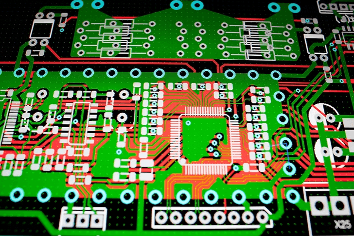
DFM centers on accurate footprints, deliberate component placement, routing strategy, thermal management, panelization, and testability so boards are compatible with automated assembly. Verified library data and correct land patterns prevent errors that cause tombstoning, solder bridges, or poor seating during pick-and-place. Placement guidelines — consistent orientation, proper edge clearance, and grouping polarized parts — reduce tape-and-reel handling issues and speed inspection. Routing choices that avoid via-in-pad on dense BGAs, preserve adequate annular rings, and provide escape routing for fine-pitch devices simplify assembly and inspection. Designing for thermal balance and providing explicit solder-mask and paste-mask definitions cut reflow defects. These practices minimize surprises and smooth the NPI cycle; the next section translates them into measurable benefits.
The complexity of surface-mount PCB assembly makes a knowledge-based advisory approach valuable — a point emphasized in earlier research.
Knowledge-Based DFM Advisor for Surface Mount PCB Assembly
Surface-mount PCB assembly continues to grow in complexity, and several studies have shown that design choices significantly affect lifecycle costs. Historically, many PCB designers lacked deep, current manufacturing knowledge, and manufacturing expertise often relied on heuristics that change with advancing processes. This research developed a knowledge-based, object‑oriented DFM advisor to help designers account for solderability, cleanliness, and reflow behavior. The system was structured with a user interface, an inference and update mechanism, and a database utility to allow maintainable rule updates and data-driven checks. Implemented on Windows in C++, the approach emphasized updateability so rules and calculations could evolve with the process.
A knowledge-based object oriented DFM advisor for surface mount PCB assembly, 1995
How DFM Guidelines Improve PCB Assembly Outcomes
Applying DFM reduces rework, increases first-pass yield, and shortens time-to-market by aligning design intent with manufacturing realities and inspection practices. For example, fixing an incorrect QFN pad in the CAD library before the prototype run can avoid a rework step that would add days and risk component damage. Industry experience shows that systematic DFM reviews at schematic-to-layout handoff and pre-production checks cut solder- and placement-related defects, improving throughput. The financial effect is lower NPI expense and more predictable schedules because fewer production iterations are needed. Clear DFM documentation also improves supplier communication, reducing ambiguity-driven delays during procurement and assembly.
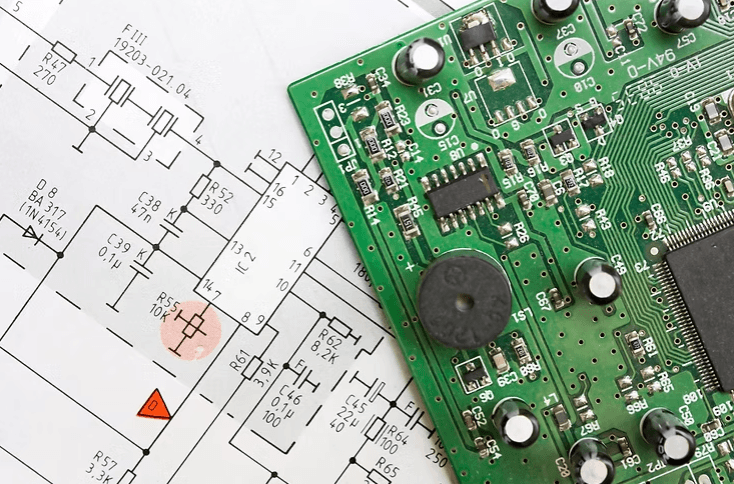
How to Prepare Accurate Design Files for PCB Assembly
Accurate design files are the single most important deliverable to an EMS — complete, consistent outputs reduce clarification loops and scrap. Essential file sets include Gerber/ODB++ for fabrication, drill and NC data, pick-and-place (centroid) files and assembly drawings for placement, an approved BOM with manufacturer part numbers and packaging details, plus test specifications for ICT/FCT. Export files with consistent units, a documented layer stack, and a clear board outline so the factory can assemble without time-consuming queries. A short pre-release checklist verifying footprints, centroid coordinates, BOM hygiene, and assembly notes prevents common pitfalls and prepares the design for panelization and stencil creation. For teams that want external validation, I-Tech E-Services LLC offers design review and file-prep support during NPI to align CAD outputs with assembly and test workflows and catch file inconsistencies before pilot runs.
Different deliverables have distinct roles during fabrication and assembly:
- Gerber/ODB++: layer-level artwork for fabrication and solder/paste-mask generation.
- Pick-and-place/centroid files: exact X/Y coordinates and rotation for placement machines.
- Approved BOMs: manufacturer part numbers and packaging details that guide procurement and reduce substitution risk.
A concise pre-release file checklist closes the loop on file integrity and cuts back-and-forth with your contract manufacturer.
What Gerber Files Are and How to Export Them Correctly
Gerbers are the layer-by-layer artwork PCB fabricators use to etch copper, define solder mask and silkscreen, and set the board outline and drill data. When exporting Gerbers, confirm correct units (mm or inches), numerical format, consistent layer names, and that the board outline and tool records are included — missing outlines or wrong units are common causes of fabrication delays. Provide a separate Excellon drill file, a README with board thickness and stackup, and a fabrication drawing with mechanical dimensions and critical tolerances. A practical Gerber export checklist removes ambiguity and prevents rebuilds that add cost and time. Verifying these details feeds directly into BOM hygiene and assembly planning, discussed next.
Tools that analyze and visualize DFM issues can help designers catch fabrication problems before they occur — a capability noted in later studies.
DFM Analysis for PCB Fabrication: Minimizing Defects and Delays
DFM analysis and 3D visualization reduce manufacturing defects and schedule risk. Tools like Valor DFMStream inspect Gerber and intelligent manufacturing files to identify design content that could lower yields or cause scrap, helping designers correct issues before fabrication. Such analysis complements manual checks and supports consistent, production-ready outputs.
Mentor Graphics Valor DFMStream
How to Build a Bill of Materials for Efficient Assembly and Procurement
A production-ready BOM includes part number, manufacturer, package, reference designator, quantity, and placement layer — plus alternate sources and Do-Not-Substitute flags where needed. Clear formatting (spreadsheet or CSV with consistent column order) prevents parsing errors and slows down quotes. Packaging details such as tape-and-reel, tube, or tray affect feeder setup, so include them. Identifying long-lead or allocation-risk items early lets procurement buffer stock or secure backup sources. A BOM hygiene checklist — matching quantities to schematic, confirming lifecycle status, and noting approved alternates — reduces line-down risk during assembly.
Best Practices for PCB Prototyping Before Full Production
Prototyping validates electrical, thermal, and mechanical assumptions before committing to volume tooling. Running a small batch on the same equipment and processes planned for production exposes DFM gaps — inadequate clearances, thermal imbalances, or placement issues — that are cheaper to fix early. Iterative test-and-refine cycles, tracked with clear revision control, lock in a design that scales without rework. The goal is a pilot-proven layout and BOM that transition cleanly into production with minimal NPI iterations. This section covers specific prototyping workflows and the role of EMS partners in accelerating learning.
What Is Design Validation and Why Does It Matter?
Design validation confirms that a PCB meets functional, reliability, and manufacturability requirements before volume release. Validation typically includes electrical testing (power-on, signal integrity, thermal imaging), mechanical fit checks, and accelerated-life or environmental stress screening where applicable. Catching a copper-weight mismatch or a marginal thermal pad before production avoids costly field returns and reputation damage. A structured validation checklist — covering electrical, thermal, mechanical, and DFM criteria — ensures nothing is skipped under schedule pressure.
How to Iterate Prototypes Effectively
Effective iteration means short cycles, tight feedback loops, and clear documentation of each change. Version-controlled CAD files and a change log linking layout revisions to test results let teams trace why adjustments were made. Grouping related fixes into a single revision rather than drip-feeding changes speeds validation and reduces confusion. Partnering with an EMS that offers quick-turn prototype builds and in-house test keeps the loop tight; I-Tech E-Services LLC provides rapid-prototype services with engineering feedback to shorten the path to production-ready designs.
Inspection and Testing Strategies for Production-Ready PCBs
Inspection and test are the gatekeepers that catch defects before shipment. A layered strategy — automated optical inspection (AOI), in-circuit test (ICT), and functional test (FCT) — balances coverage and cost. Defining test points and access during layout (not after) ensures fixtures can probe critical nodes. Clear pass/fail criteria and traceability records support root-cause analysis when defects occur. This section details each inspection stage and how to balance coverage against cost.
What Are Common Inspection Methods in PCB Assembly?
AOI uses cameras and algorithms to detect solder defects, component placement errors, and polarity issues at line speed. X-ray inspection is used for hidden joints under BGAs, QFNs, and leadless packages where optical methods cannot see. Manual visual inspection (MVI) remains a backstop for complex or low-volume boards where fixture cost is not justified. Each method has trade-offs in speed, coverage, and cost; combining them in the right sequence maximizes defect capture without unnecessary expense.
How to Plan Electrical Testing for High Yield
Electrical testing includes ICT for node-level shorts, opens, and component-value verification, and FCT for system-level behavior under load. Designing with adequate test pads, consistent grid spacing, and accessible probe points lowers fixture cost and improves coverage. Defining test cases that mirror real-world operating conditions catches marginal failures that might escape bench tests. Tracking first-pass yield and pareto-charting failure modes feeds continuous improvement and reduces long-term cost.
How to Control Costs and Mitigate Risks in PCB Manufacturing
Cost and risk control starts in design and extends through supplier selection and production ramp. Major cost drivers include component scarcity, PCB layer count, fine-pitch assembly, and test-fixture development. Mitigation tactics — early sourcing, alternate-part qualification, and DFM reviews — reduce surprises. This section maps the cost levers and risk factors teams should monitor.
What Are the Major Cost Drivers in PCB Assembly?
Component cost and availability often dominate; long-lead or allocation-constrained parts can stall production. PCB fabrication cost rises with layer count, tight tolerances, and exotic materials (high-Tg, RF laminates). Assembly cost scales with placement count, fine-pitch devices, and mixed SMT/THT processes. Test-fixture NRE and inspection time add overhead; designing for testability reduces both. Understanding these drivers lets teams make trade-offs that balance performance and budget.
How to Mitigate Supply-Chain and Quality Risks
Supply-chain risk mitigation includes qualifying second sources, buffering safety stock on critical parts, and monitoring end-of-life notices. Quality risk mitigation means locking in DFM reviews, specifying IPC acceptance classes, and requiring traceability from component lot to finished board. Contractual terms — clear quality specs, inspection rights, and corrective-action requirements — protect against disputes. A risk register that tracks component availability, supplier performance, and defect trends keeps issues visible and actionable.
How to Evaluate and Select a Contract Manufacturer
Choosing the right EMS partner affects quality, cost, and schedule throughout the product lifecycle. Evaluation criteria include certifications (AS9100, ISO 13485:2016 certified by NQA, ITAR), equipment capability, engineering support, and communication responsiveness. Site visits, reference checks, and pilot builds reveal operational reality beyond sales presentations. This section provides a structured vendor-evaluation framework.
What Certifications and Capabilities Matter?
Industry-specific certifications signal process maturity: AS9100 for aerospace, ISO 13485:2016 certified by NQA for medical, ITAR registration for defense. Equipment lists — placement machines, reflow ovens, AOI, X-ray, ICT fixtures — indicate capacity and precision. Engineering resources for DFM review, test development, and NPI support shorten ramp time. A vendor that can handle your product mix (board complexity, volume, test requirements) without overloading its lines delivers more reliable schedules.
How to Structure Vendor Communication for Smooth NPI
Clear, frequent communication prevents misalignment during NPI. Define a single point of contact on each side, establish regular status calls, and use shared dashboards for BOM status, engineering questions, and schedule updates. Early file reviews and DFM feedback sessions catch issues before they become production problems. Documenting decisions and change orders maintains accountability and supports root-cause analysis if issues arise. I-Tech E-Services LLC emphasizes proactive NPI communication to align customer expectations with production realities and reduce time-to-market.
Partner with I-Tech E-Services for Your Next PCB Project
At I-Tech E-Services LLC, we combine AS9100D, ISO 13485:2016 (certified by NQA), and ITAR registration with hands-on engineering support to guide your design from prototype through production. Our capabilities span PCB assembly, cable and wire harnesses, box builds, and comprehensive testing — all under one roof in the U.S. Whether you need a quick-turn prototype, DFM review, or turnkey production, our team is ready to help you reduce program risk and accelerate time-to-market.
Contact us today to discuss your project requirements and get a quote.