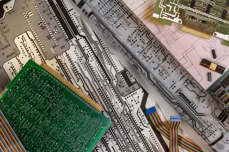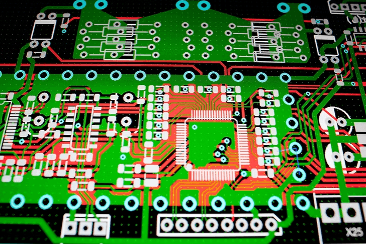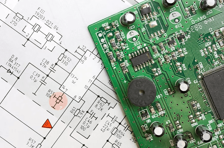



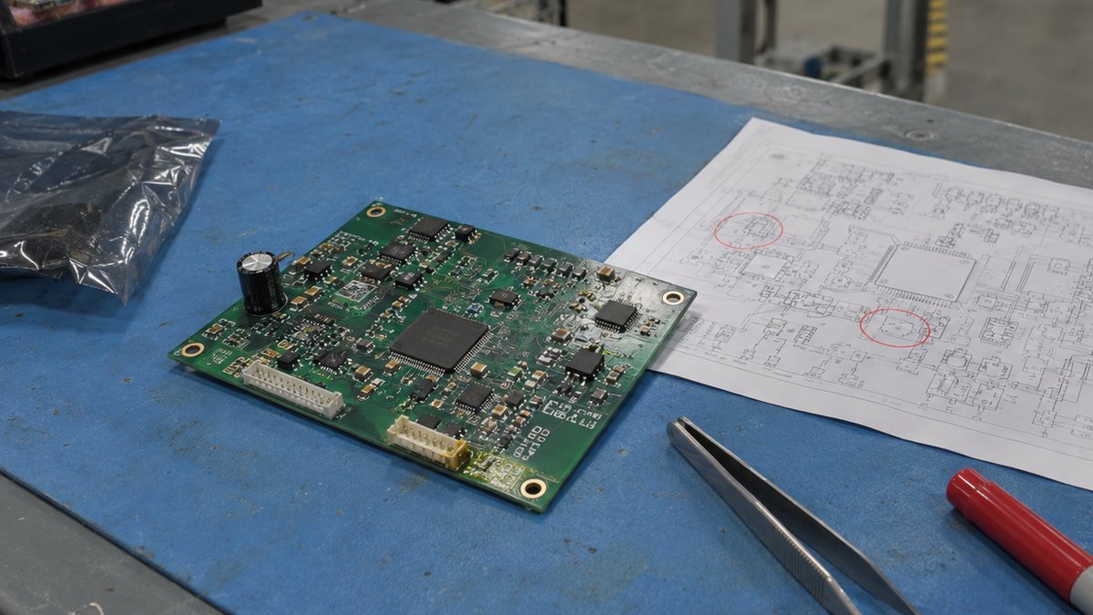
A PCB DFM checklist is the fastest way to keep layout mistakes from stalling your first article build. Most first-article delays trace to a short list of layout and data-package problems: land patterns that don't match the purchased part, polarity marks hidden under components, missing fiducials, parts crowding board edges and score lines, unbalanced copper on small passives, open vias in pads, solid paste on QFN thermal pads, unbuildable solder mask webs, tall parts that block inspection, heavy parts on the wrong side, no test access, and a centroid or BOM that disagrees with the layout. Each is cheap to fix in CAD and expensive to fix after boards are built.
The checklist below is written for the engineers and program managers who release boards to a contract manufacturer. It does not replace your own design review: your layout team owns the design and its sign-off. Use it as a pre-release pass on the issues that most often turn into holds, rework, or engineering questions when the first boards are built.
Why layout mistakes surface at first article
First article is the first time a design meets a real production process: a stencil, a pick-and-place program, a reflow profile, automated optical inspection (AOI), and electrical test. A layout that passes your CAD design-rule check (DRC) can still be hard to build, because DRC verifies electrical and fabrication rules such as spacing, annular ring, and clearances. It does not model how solder paste, placement heads, and inspection cameras behave on the floor. The gap shows up as tombstoned resistors, bridged fine-pitch leads, voided thermal pads, or a placement program that cannot be finalized because the files disagree.
The cost is rarely the rework itself. It is the schedule: a hold while questions go back and forth, a board re-spin, a new stencil, and on aerospace programs, a partial or full first article inspection (FAI) to SAE AS9102 when a design change affects the part. One avoidable re-spin can add weeks to a prototype-to-production program. The cheapest place to catch these issues is before release, which is exactly what a PCB DFM checklist is for.
The PCB DFM checklist: 12 layout red flags
Each item below is phrased as the question to ask before you release Gerbers or ODB++, followed by why it matters at first article and what to change.
1. Do your land patterns match the parts you are actually buying?
The most common footprint error is a land pattern drawn for a different package variant than the part on the BOM: a QFN with a different exposed-pad size, an SOT-23 with a different pinout, or a connector from the same family with its mounting pegs in a different place. Build footprints from the manufacturer's datasheet for the exact part number, and size pads to IPC-7351, the land pattern standard, at the density level that suits your assembly. When the BOM lists alternates, confirm every approved alternate fits the same footprint. A mismatched land pattern means hand rework at best and a re-spin at worst.
2. Can the assembler still see polarity and pin-1 marks after placement?
Polarity marks that sit under the component body disappear the moment the part is placed, so neither the operator nor AOI can confirm orientation. Put diode, LED, electrolytic capacitor, and IC pin-1 indicators where they stay visible beside the placed part, and use one convention across the board, such as always marking the cathode. Keep silkscreen off pads; the fabricator will clip it, often taking the mark with it. Repeat the same marks on the assembly drawing so orientation never depends on guesswork.
3. Does the board have enough fiducials, in the right places?
Fiducials are the optical targets the pick-and-place machine uses to correct for board position, rotation, and stretch. Without them, placement accuracy suffers on fine-pitch parts. Place at least three global fiducials in a non-symmetric pattern near the board corners, plus local fiducials beside fine-pitch QFPs and BGAs. A typical fiducial is a 1 mm bare copper dot with a mask-free clearance of roughly two to three times its diameter. If boards ship in a panel, add fiducials to the panel rails as well.
4. Are parts too close to the board edge, V-scores, or breakaway tabs?
Assembly lines carry boards on conveyor rails, so components within roughly 3 to 5 mm of an edge either need panel rails added or cannot be placed by machine. Depaneling adds a second risk: flexing at a V-score or breakaway tab can crack multilayer ceramic capacitors, and those cracks often pass test and fail later in the field. Keep ceramic capacitors and other brittle parts back from break lines, orient their long axis parallel to the break line, and agree on the panel design with your manufacturer before release.
5. Are small passives tied to copper pours without thermal relief?
When one pad of an 0402 or 0201 resistor or capacitor connects straight into a ground plane and the other connects to a thin trace, the two ends reach reflow temperature at different times. The pad that wets first pulls the part upright, a defect known as tombstoning. Use thermal-relief spokes on plane connections, keep pad sizes and trace entries symmetrical, and avoid running a wide trace into only one end of a small chip part. It is one of the easiest first-article defects to prevent and one of the most tedious to rework.
6. Are there open vias inside component pads?
An unfilled via in a pad acts like a drain: molten solder wicks down the barrel, leaving a starved joint on top and solder on the far side of the board. Under BGAs and very fine-pitch parts, via-in-pad is often unavoidable, so specify it properly as filled and capped (plated over), the structure IPC-4761 classifies as Type VII. Where via-in-pad is not required, move the via off the pad with a short trace and keep a solder mask dam between them. Call out via treatment explicitly in the fabrication notes rather than leaving it to interpretation.
7. Is the QFN thermal pad printed as one solid block of paste?
A full-coverage stencil aperture on a large exposed pad deposits too much solder, which can float the package, bridge the perimeter leads, and trap voids. IPC-7093, the design and assembly guide for bottom-termination components such as QFNs, covers the alternatives. Segment the aperture into a windowpane pattern that typically prints around 50 to 80 percent coverage, and treat thermal vias in the pad so they do not steal solder. Stencil design is usually your manufacturer's call, but the pad and via layout that makes it work is set in CAD.
8. Can the fabricator actually build the solder mask webs at your pitch?
On fine-pitch QFPs, QFNs, and connectors, the strip of solder mask between adjacent pads is what keeps solder from bridging. If the gap is narrower than the fabricator can reliably hold, often around 3 to 4 mil (0.075 to 0.1 mm), they remove the webs and open the whole row, and bridging risk rises at assembly. Check pad-to-pad spacing against your fabricator's minimum mask web, choose solder-mask-defined or non-solder-mask-defined pads deliberately, and make sure the mask expansion in your CAD library matches what the fabricator expects.
9. Do tall parts block inspection cameras or rework tools?
Tall electrolytic capacitors, inductors, and connectors cast shadows that hide nearby joints from AOI cameras, and they leave no room for a rework nozzle or soldering iron. Keep a clear zone of a few millimeters around BGAs so they can be reworked, keep small passives off the shadowed side of tall parts, and consider the viewing angle for gull-wing and J-lead joints. Hidden joints still need verification; BGAs and QFNs rely on X-ray, which we cover in our guide to AOI vs. X-ray inspection for BGA and QFN.
10. Are heavy or through-hole parts on the wrong side of the board?
On a double-sided reflow board, parts on the first side ride upside down through the second reflow. Small passives stay put, but heavy inductors, large connectors, and big ICs can drop off unless they are glued or moved. Through-hole parts add another constraint: if they are wave or selective soldered, bottom-side SMT parts near their leads need clearance for the solder nozzle or a pallet, or the joints must be hand soldered. Put heavy and through-hole parts on the primary side where you can, and group through-hole parts so one process can reach them all.
11. Can a test probe reach the nets that matter?
Every net you want electrically tested needs exposed copper a probe can touch: a test pad, a via, or an accessible component termination. Bed-of-nails fixtures prefer targets of about 1 mm on a 2.54 mm (100 mil) grid, ideally all on one side. Flying-probe testers are more forgiving and need no fixture, which suits prototypes and low volumes, but they still cannot reach pads under components or behind tall parts. Agree on the test strategy before layout is frozen, then reserve access for power rails, critical signals, and programming headers.
12. Do the centroid, BOM, and drawings agree with the layout?
Many first-article holds are not geometry at all; they come from a data package that contradicts itself. The pick-and-place (centroid) file lists a part the BOM marks do-not-populate (DNP), a reference designator appears in one file but not the other, the assembly drawing is a revision behind, or rotation values follow a CAD convention the assembler has to guess at. Export Gerbers or ODB++, drill, centroid, BOM, and assembly drawing from the same revision, mark every DNP in both the BOM and the drawing, and state the IPC acceptance class and any special requirements in the notes.
Common mistakes when using a PCB DFM checklist
- Running it after release. A checklist run after Gerbers are at the fabricator only documents the problems. Run it while the layout can still change.
- Treating a clean DRC as assembly-ready. Design-rule checks confirm fabrication and electrical rules, not paste, placement, inspection, or test.
- Fixing on the floor instead of in CAD. Hand rework can save a first-article build, but if the layout is not corrected, the same defect returns on every production lot.
- Not feeding first-article findings back. Capture every hold, question, and rework from first article, and close each one in the next revision before volume.
- Leaving decisions to interpretation. Via treatment, acceptance class, surface finish, and DNPs belong in the release notes, not in an email thread.
How i-TECH e-Services builds your first article
i-TECH e-Services is a U.S. contract electronics manufacturer in Norcross, Georgia, building prototypes through production for aerospace and defense, medical, and industrial OEMs under AS9100D and ISO 13485:2016. Design ownership and sign-off stay with your engineering team. We build to your released documentation, and when something in the package does not line up, our team asks early so it is resolved before the build instead of discovered after it.
- Quick-turn first builds. Prototype assembly ships in 5 to 7 business days once files and parts are in hand, with a 3-day express option and a seamless transition to production.
- Class 3 workmanship. PCB assembly is soldered to J-STD-001 and inspected to IPC-A-610 Class 3.
- Inspection and test that confirm the build. 3D AOI (Parmi), X-ray (Glenbrook) for hidden BGA and QFN joints, SPEA flying-probe test, and functional test, detailed under quality and testing.
- Rework when it is needed. BGA rework on Air-Vac equipment, along with the rest of our manufacturing capabilities.
For a broader look at moving a design from prototype to volume, read preparing your PCB design for smooth assembly. Ready to build? Request a prototype quote and send your files to our team.
Bottom line
A PCB DFM checklist turns first article from a discovery exercise into a confirmation. Check land patterns against the parts you are buying, keep polarity marks visible, add fiducials, clear the edges, balance copper on small passives, fill and cap vias in pads, segment QFN paste, respect mask web limits, leave room to inspect, rework, and test, and release one consistent data package. Twelve questions asked before release take an afternoon; the same twelve answered after first article can cost a re-spin, a new stencil, and weeks of schedule.